Optical chiplets for AI address a problem that is easy to overlook: powerful processors must move enormous amounts of information before they can do useful work. A faster calculation does not help much if the next piece of data arrives too late. That makes the connections between chips part of the AI performance story.
On October 20, 2026, NTT and its partners announced a manufacturing research project for photonics-electronics convergence devices. The news is about making an emerging connection technology practical to produce. It is not the launch of a consumer AI product or a claim that today’s servers have become all-optical computers.
The distinction that matters: the project targets manufacturing productivity, not a tenfold increase in AI model speed. This article explains the announcement and its implications; we have not independently tested the proposed hardware.
What was announced today?
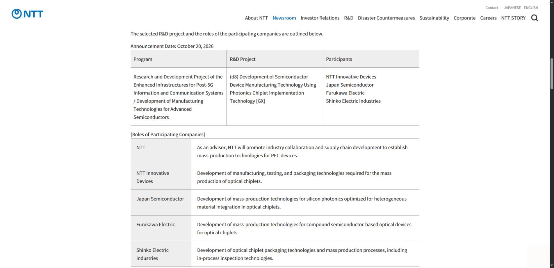
The official NTT announcement says a proposal led by NTT Innovative Devices was selected under a NEDO semiconductor manufacturing R&D program. Japan Semiconductor, Furukawa Electric and Shinko Electric Industries are the other participating companies, with NTT advising.
The group plans a pilot production line and targets more than ten times the manufacturing productivity of current R&D-stage processes. Its work spans optical devices, silicon photonics, testing and packaging. These are development objectives, rather than evidence of an already completed commercial rollout.
An optical chiplet, in plain language
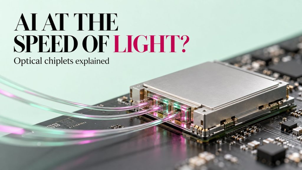
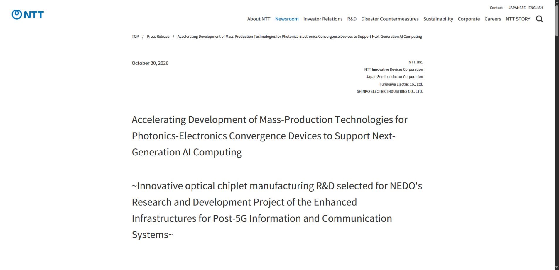
A chiplet is a smaller semiconductor building block that works with other components in a larger package. An optical chiplet adds a way to communicate using light. Electronic circuits handle electrical signals, while photonic components help transmit or receive information optically.
Think of a processor as a busy workshop. Its machines may be fast, but they still need materials delivered between stations. Improving those delivery routes can help the whole workshop. The analogy has limits: an optical connection still needs transmitters, receivers and a suitable physical path, rather than moving information for free.
The word “optical” describes how information travels along a connection. It does not mean every calculation takes place in light. A system can combine conventional electronic computing with optical communication, just as a network can combine different kinds of links.
Why moving data matters to AI
An AI system is more than one processor executing one instruction stream. It includes memory, accelerators, communication links, storage and software that coordinates work. When a task is spread across devices, the system must exchange information at the right time.
There are several distinct limits. Bandwidth is how much information a connection can carry over time. Latency is the delay before a transfer or response arrives. Energy efficiency concerns how much work is completed for the energy consumed. Improving one measure does not automatically improve all the others.
Our AI networking explainer discusses the wider communication problem. Optical chiplets focus closer to the computing hardware; they should not be treated as interchangeable with every networking upgrade.
The benefit depends on the bottleneck
Imagine two hypothetical workloads. The first spends much of its time waiting for transfers between processing devices. The second mostly waits for data in local memory. A better inter-chip link could matter much more to the first. The same hardware improvement can therefore produce different application results.
This is why a single headline number rarely tells the whole story. A link benchmark measures a connection. A system benchmark measures a larger arrangement. An application benchmark measures a particular task under particular settings. Those results answer different questions.
What the key terms do—and do not—tell you
| Term | Useful meaning | Do not assume |
|---|---|---|
| Optical chiplet | A component supporting optical communication | All computation uses light |
| Photonics-electronics convergence | Combining photonic and electronic functions | Electronics disappear |
| Pilot production line | A step toward repeatable manufacturing | Large-scale deployment is complete |
| Manufacturing productivity | Output relative to the production process | The same multiplier applies to AI speed |
Keep the unit and baseline attached to every comparison. “Faster” might refer to a data link, a manufacturing step or a complete application. Without that context, readers can mistake a real engineering goal for a much broader performance promise.
Why manufacturing is a major part of the story
A laboratory demonstration answers whether an idea can work under particular conditions. Manufacturing asks a different set of questions: can it be built repeatedly, tested efficiently and integrated with other parts at an acceptable cost? A promising component must pass both kinds of test.
Packaging is particularly important because a semiconductor does not operate in isolation. It needs physical connections, power delivery and thermal management. A package must hold components in the correct arrangement and remain reliable while operating conditions change.
Testing also affects whether a technology can scale. Finding a defective part early may avoid spending more manufacturing effort on an assembly that cannot be used. A production process needs ways to detect faults, understand their causes and improve consistency.
For readers following the industry, this creates a useful change of emphasis. Watch the path from a working prototype to repeatable production, rather than looking only for the next peak-performance demonstration. Progress in that path can be commercially meaningful even when it does not produce a dramatic chatbot demo.
Could optical chiplets reduce AI energy use?
They are intended to address communication efficiency, but whole-system energy savings require whole-system evidence. A complete deployment also includes processors, memory, power conversion, cooling and other equipment. An improvement in one part should not be reported as the same percentage reduction in the entire facility.
A useful measure is energy per completed task at a stated quality level. Compare systems running the same workload with clear boundaries around what is measured. The number is less meaningful if one test excludes cooling or uses a different task configuration without saying so.
Our AI data center energy guide explains why electricity demand is broader than an individual chip. Better efficiency can coexist with rising total consumption when the amount of computing grows.
Read efficiency claims carefully. Ask what was measured, at what scale and against which baseline. A component improvement is useful evidence about that component; it does not establish every benefit of a future data center.
What this means for people using AI tools
There is no new optical-chiplet setting to switch on in an ordinary assistant. Infrastructure changes usually reach users through the service they already use. Whether a service becomes faster or cheaper depends on deployment decisions, software and pricing, as well as hardware.
For now, evaluate an AI tool through results you can observe: task accuracy, response time, reliability and cost. A provider’s hardware announcement does not establish the quality of its answers. Better information transport cannot by itself eliminate hallucinations or guarantee useful reasoning.
What businesses should ask before planning around it
A research announcement can inform a technology watchlist without becoming an immediate purchase requirement. Teams should connect the proposed improvement to a measured constraint in their own workload. Otherwise they risk optimizing a part of the system that is not holding them back.
- Which workload is limited by communication today?
- What application-level test would show a meaningful improvement?
- What equipment, software and packaging changes would adoption require?
- How will reliability, maintenance and replacement be assessed?
- Which commercial milestones remain unconfirmed?
These questions help separate exploration from commitment. They also encourage comparisons that survive changes in vendor terminology. The decision should follow demonstrated workload value and operational fit, rather than the most exciting name for an underlying technology.
Three signals to watch next
1. Repeatable production results
Look for evidence that the process works consistently across many devices, rather than a selected example. Yield, inspection and reliability information can be more useful at this stage than another isolated speed record.
2. Integration into a complete system
Watch how the components connect to the rest of the platform. A successful integration needs compatible hardware and software, practical power and cooling arrangements, and a clear account of what was measured.
3. Application-level comparisons
The strongest practical comparison runs a representative task under disclosed conditions. It reports performance and energy alongside correctness or output quality where relevant. This helps readers judge whether a link-level improvement translates into useful work.
Frequently asked questions
Do optical chiplets replace GPUs?
Not simply. They concern communication components and integration. A system can use optical connections alongside electronic processors. Replacing a communication path is different from replacing the processor that performs the computation.
Does NTT’s tenfold target mean AI will become ten times faster?
No. The announcement’s target refers to manufacturing productivity relative to current R&D-stage processes. It should not be rewritten as a claim about model speed, answer quality or total data center energy savings.
Is this technology already available to ordinary users?
This announcement describes a manufacturing development project. It does not provide a consumer product to buy or a feature to enable in an AI application. Availability in a particular service requires separate confirmation.
Are optical chiplets the same as optical computing?
The terms overlap in broader discussions of photonics, but they are not interchangeable. Using light to communicate between components is different from using photonic operations to perform computation. Check which function a specific announcement describes.
The practical takeaway
Optical chiplets for AI are worth following because the cost of moving information matters alongside the cost of calculation. Today’s NTT news focuses on the difficult step of making that technology repeatable to manufacture. Follow production and system-level evidence before translating the goal into claims about everyday AI performance.
Source and review: NTT’s October 20, 2026 joint announcement supports the project details. The explanations, hypothetical workload example and evaluation questions are editorial analysis. Reviewed October 20, 2026; project plans can change.